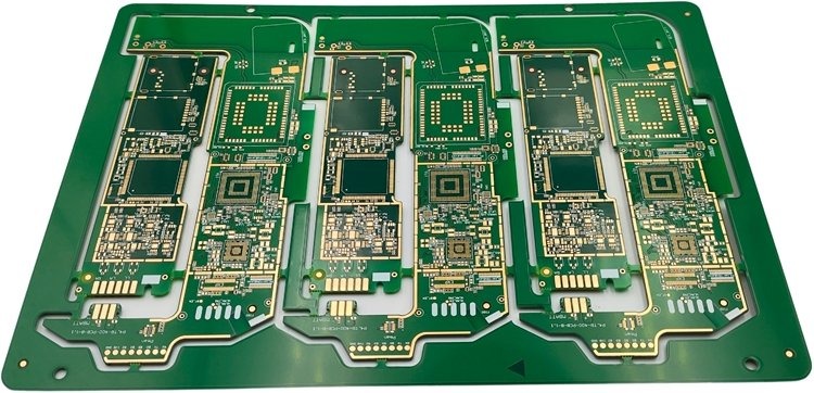
Modern electronics increasingly depend on PCBs that can accommodate dense routing, complex multilayer structures, and demanding electrical requirements without making the overall product unnecessarily large. For communications equipment, EMS projects, and industrial control systems, the manufacturing partner must be capable of handling more than conventional multilayer fabrication.
Choosing the right HDI PCB manufacturer means evaluating the supplier’s actual technical capabilities, engineering support, production timelines, and ability to manufacture complex board structures consistently.
Why HDI Manufacturing Requires More Than Standard PCB Production
HDI designs often combine multiple routing layers and build-up structures to provide greater interconnection density. As the design becomes more complicated, manufacturing decisions involving layer configuration, fine-line routing, stack-up, and impedance become increasingly important.
For purchasing teams and engineers, the key question is not simply whether a supplier offers HDI PCBs. It is whether the manufacturer can support the specific structure and electrical requirements of the project.
This is particularly important when a board includes:
- High layer counts
- Dense component areas
- Fine-line traces and spaces
- Controlled-impedance requirements
- Multiple HDI build-up stages
- Complex multilayer routing
- Tight product size constraints
A capable manufacturer should be able to review these requirements before production and identify potential manufacturability issues early.
HDI Structures: 1+N+1, 2+N+2, and 3+N+3
One of the most important capabilities to evaluate is the manufacturer’s experience with different HDI build-up structures.
HDI designs may use configurations such as 1+N+1, 2+N+2, and 3+N+3. The appropriate structure depends on the routing requirements, component density, layer arrangement, and overall electrical design.
A 1+N+1 structure can suit designs that require a comparatively straightforward build-up approach, while 2+N+2 and 3+N+3 structures can support progressively more complex interconnection requirements.
The ability to manufacture multiple HDI structures gives engineers greater flexibility when optimizing a board rather than forcing every design into the same construction method.
Complex Multilayer PCB Capability
HDI is often used alongside high layer counts when a design contains extensive routing requirements. Therefore, layer capability should be evaluated together with HDI structure capability.
FastTurnPCB supports PCB manufacturing with up to 50 layers, allowing complex designs to be developed using substantial multilayer configurations.
For an EMS company or electronics manufacturer, this can be particularly useful when different projects require different board constructions. Instead of selecting a supplier only for simple HDI prototypes, purchasing teams can consider whether the manufacturer has the technical range to support increasingly complex products as they move toward production.
The supplier should also understand how the layer structure affects manufacturability, material selection, stack-up design, and electrical performance.
Fine-Line Manufacturing for Dense Routing
Fine-line capability is another practical factor that should be considered when selecting an HDI supplier.
As routing density increases, designers may need smaller trace widths and spaces to fit the required connections into limited PCB areas. FastTurnPCB supports line width and spacing down to 2.5/2.5 mil.
Fine-line manufacturing requires consistent fabrication control because variations in trace geometry can affect both manufacturability and electrical performance.
When evaluating a supplier, engineers should therefore look beyond a stated minimum capability. They should also consider whether the manufacturer has an engineering process for reviewing the design and confirming that the selected line/space configuration is appropriate for the complete stack-up.
Impedance Control and Stack-Up Engineering
Complex HDI boards frequently contain high-speed signal paths where controlled impedance is an important design consideration.
Impedance is affected by several manufacturing variables, including:
- Trace width
- Dielectric thickness
- Copper thickness
- Material characteristics
- Distance between signal and reference layers
- Overall stack-up configuration
FastTurnPCB supports an impedance tolerance of ±5%.
However, impedance control should begin during engineering review rather than being treated as a final-stage manufacturing check. A properly planned stack-up can help ensure that trace geometry and dielectric relationships support the required electrical characteristics.
For this reason, buyers should ask an HDI supplier how stack-up requirements are reviewed before manufacturing and whether engineering support is available when adjustments are needed.
DFM and Engineering Review
For complex HDI boards, Design for Manufacturability (DFM) is especially valuable because manufacturing problems can become more difficult and expensive to correct after fabrication begins.
A practical supplier evaluation should include questions such as:
- Does the manufacturer provide DFM review?
- Can the engineering team suggest design adjustments?
- Can the supplier review the stack-up?
- Can impedance requirements be considered during engineering?
- Can panelization be optimized for production?
- Can the supplier respond quickly when design questions arise?
FastTurnPCB provides DFM support along with stack-up guidance, design adjustment suggestions, and panelization optimization.
Early engineering communication can help identify potential problems before they affect production schedules. It also gives purchasing teams greater confidence that the supplier understands the technical requirements rather than simply accepting files and starting fabrication.
HDI for Communications Equipment
Communications products are a major application area for complex PCB manufacturing. Network equipment, wireless systems, communication modules, and other advanced electronics can require dense routing within constrained physical dimensions.
For these applications, HDI structure, fine-line capability, and impedance control may need to be considered together.
A supplier capable of supporting multiple HDI structures can give communication-product engineers more options when balancing routing density, layer count, and electrical performance.
HDI for EMS Manufacturing
EMS companies often manufacture products designed by external customers, meaning they may need to work with a wide variety of PCB designs.
This makes manufacturing flexibility particularly important. An EMS purchasing team may encounter a simple 1+N+1 design for one project and a considerably more complex 2+N+2 or 3+N+3 structure for another.
A supplier that supports multiple HDI configurations, high layer counts, fine-line manufacturing, impedance control, and DFM can reduce the need to search for a different PCB source every time project complexity changes.
Lead time is also important. FastTurnPCB states an approximate 10-day manufacturing time for HDI boards, although the actual schedule depends on the specific design and production requirements.
HDI for Industrial Control Systems
Industrial control equipment can also involve complex PCB designs containing processors, communication interfaces, sensors, control circuitry, and other electronic functions.
These systems may require dense routing while maintaining predictable electrical performance and reliable multilayer construction.
For industrial applications, purchasing teams should evaluate whether the PCB supplier can maintain consistency across prototypes and production quantities. Engineering support is equally important because a small design adjustment made before manufacturing can prevent larger production problems later.
What to Evaluate When Choosing an HDI Supplier
The most important evaluation should focus on manufacturing capabilities rather than general HDI terminology.
Look for a supplier that can support:
- HDI structures: 1+N+1, 2+N+2, and 3+N+3.
- Complex multilayer boards: Capability up to 50 layers can provide greater design flexibility.
- Fine-line manufacturing: Confirm the supplier can support the required trace width and spacing, including 2.5/2.5 mil when needed.
- Impedance control: A defined tolerance such as ±5% should be evaluated against project requirements.
- Engineering support: DFM, stack-up review, design adjustments, and panelization optimization can reduce manufacturing risk.
- Lead-time capability: HDI production schedules should be realistic for the board’s structure and complexity.
This type of evaluation helps buyers compare suppliers based on measurable manufacturing capabilities rather than simply choosing a company because it advertises HDI production.
Conclusion
Selecting an HDI supplier is ultimately a technical manufacturing decision. The right partner should be able to support different build-up structures, complex multilayer configurations, fine-line routing, controlled impedance, and engineering review.
For communications equipment, EMS manufacturing, and industrial control systems, these capabilities can make a significant difference when moving from a challenging PCB design to a manufacturable product.
By evaluating HDI structure capability, layer count, 2.5/2.5 mil line and space, ±5% impedance tolerance, DFM support, and realistic lead times, purchasing teams and engineers can make a more informed supplier decision.
With support for 1+N+1, 2+N+2, and 3+N+3 HDI structures, up to 50-layer PCBs, fine-line manufacturing, and engineering assistance, FastTurnPCB can support complex PCB manufacturing requirements from engineering review through fabrication.